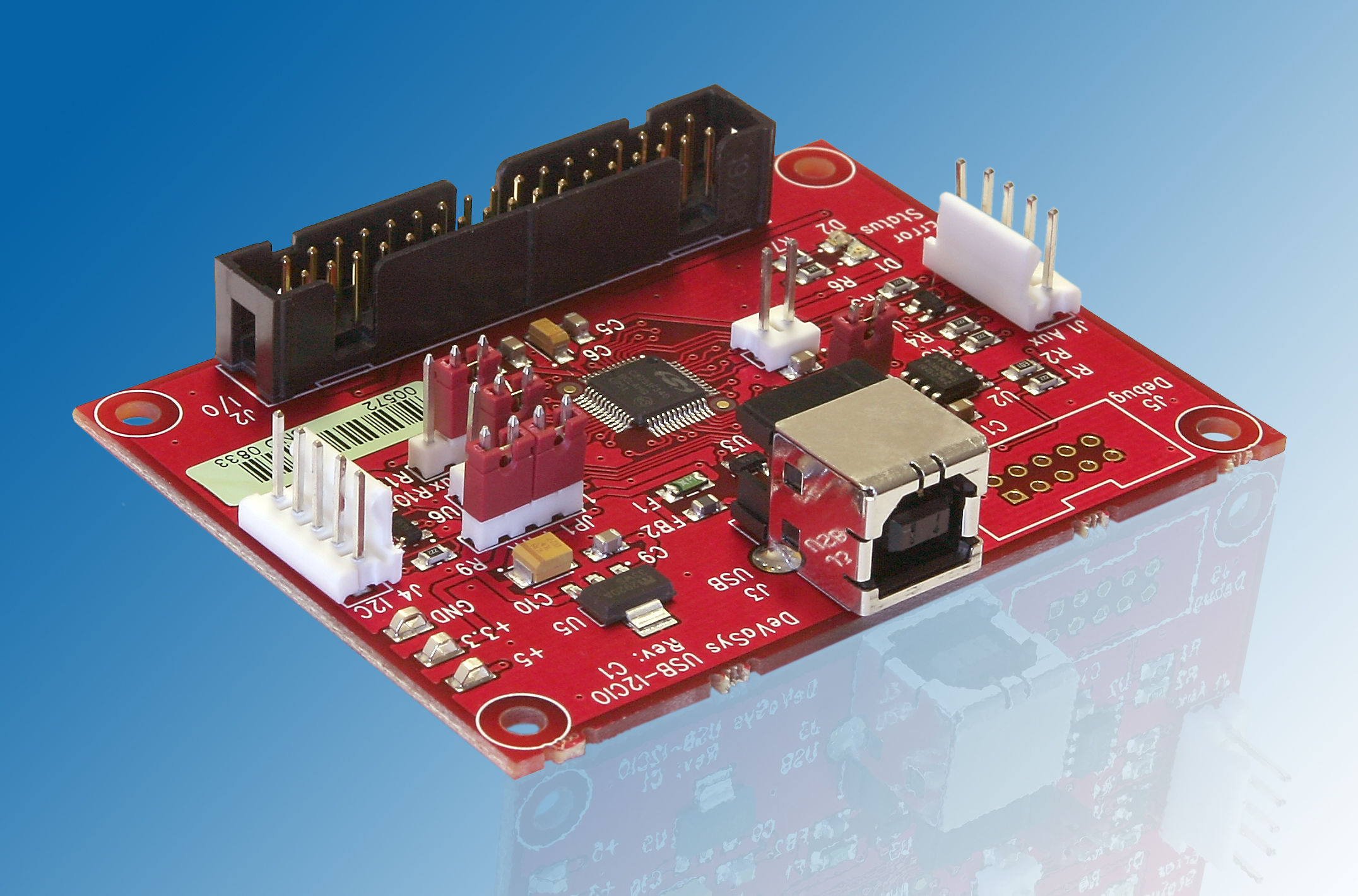
 | It's red! The Rev. C1 board uses red solder mask to make it easy to distinguish between Rev.
C1 and Rev. Bx boards (which are blue). |
| It's RoHS compliant (lead free)! We may have some documentation
and/or labeling work to do, but the p.c.b., all components, and the assembly
process, all conform to the requirements. |
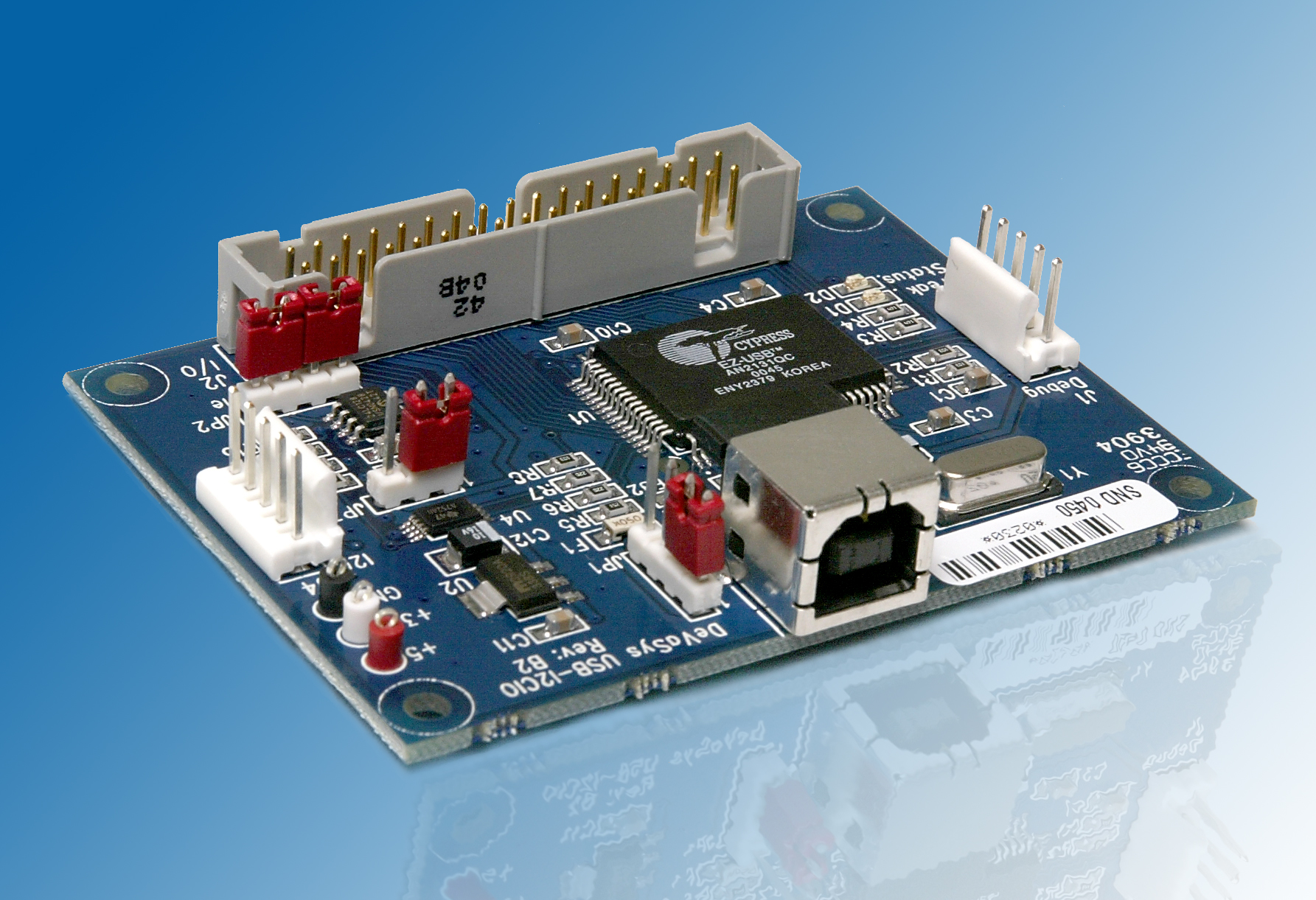
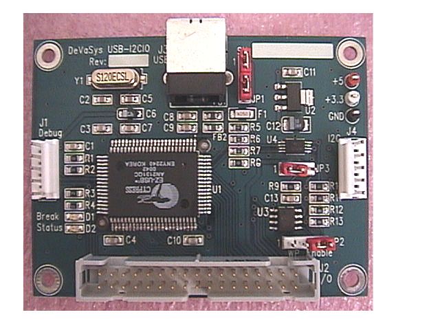
| Changed the micro-controller from the obsolete Cypress AN2131QC to the
Silicon Labs C8051F340. We are very excited about this new micro, as
it solves a number of issues with the old micro, while providing greatly
enhanced speed and functionality. |
| Changed the three voltage test-points from through-hole to surface
mount. |
| Enhanced the ESD protection using 3 separate devices for USB D+/D-, I2C SCL/SDA signals,
and Auxiliary connector signals. |
| Moved onboard I2C eeprom to it's own I2C bus segment to solve I2C
address conflict issues. |
| Renamed "Breakpoint" LED function to "Error" for use as an error
indicator. |
| Changed pin-out and function of the J1 header from "Debug" to
"Auxiliary". This header is intended to eventually provide for
enhanced functionality, like a a second I2C channel, or possibly support for
some 1-wire interfaces. The Debug header was largely unused by
customers, so we do not anticipate this change to be a problem for most
customers. |
| Replaced the Data Bus signals on the J2 header with 8 more general
purpose I/O pins. These pins will eventually be configurable to
support other configurable functions such as SPI bus, another I2C channel,
etc. |
| Moved the configuration headers and jumpers around (see schematics for
circuit details). |
![[Company Logo Image]](images/Logomed.jpg)


