| It's Blue! The Rev. B board uses Blue Solder Mask to make it easy to distinquish between Rev. A and Rev. B boards. |
| Eliminated one of the ground test points. |
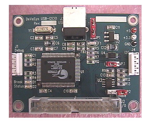
| Moved all test points to edge of board for easier access. |
| Changed regulator circuit capacitors to better comply with component datasheet and USB specification. |
| Added Ferrite Beads to Vusb and Ground signals from USB connector (EMI filtering). |
| Added ESD protection device to USB D+/D- and I2C SCL/SDA signals (ESD hardening) |
| Added resettable fuse to Vusb signal to provide some protection for upstream equipment. This fuse goes to high impedance state
in an overcurrent condition, and automatically returns to low impedance state when it cools. |
| Added write protection for I2C eeprom. The write protection can be enabled or disabled via a jumper. |
| Changed eeprom enable jumper from a 2 pin to a 4 pin header, to include write protect feature. |
| Added pullup resistor for I2C interrupt signal. |
| Changed "Status" LED to surface mount component. |
| Added "Breakpoint" LED to show state of "Breakpoint" signal from AN2131QC. |
| Changed P.C.B. footprint and schematic pinout for the two 5 pin headers (Debug and I2C). The signals are all still in the same
physical locations as the Rev. A board, only the references to pin numbering have been changed (to match the actual AMP reference on
the mating connector). In other words, pin 1 is now pin 5... but pin 5 is where pin 1 used to be... and has the same signal on it. |
| Increased I/O connector from 26 to 34 pins. The 34 pin connector is exactly 8 pins larger, and is situated such that the center
26 pins occupy the same physical space as the orignal 26 pin header (4 extra pins on each end). All but two of the original I/O signals
are in their exact same physical space. The I2C signals have been replaced with CLK24 and RESET, and the additional 8 pins
are for the data bus signals. This change provides support for the "Fast FIFO Transfer" operations of the AN2131QC, which will allow
the board to transfer data to/from external circuitry at full USB 1.1 rates (nearly 1MB/sec on an unloaded bus). |
![[Company Logo Image]](../../images/Logomed.jpg)